AnasSarkiz/ble-pedometer
This code defines and configures various electronic hardware components such as surface-mount resistors, crystals, diodes, transistors, connectors, and switches with their physical footprints, schematic symbols, and 3D CAD models for PCB assembly.
- Version
- 1.0.7
- License
- unset
- Stars
- 0
DATASHEET_AUDIT.md
# Datasheet audit

Checked against official manufacturer documents during this design pass: TI CC2340R5 datasheet Rev F and hardware design guide SWRA834A; BQ25186 SLUSF69A; TPS7A02 SBVS277C; BQ27427 SLUSCD5B and technical reference SLUUCY5B; Bosch BMA400 Rev 2.3; Abracon ABM11W data; and Johanson 2450AT18A100 data.

## U1 — CC2340R52E0RGER, 24-pin RGE VQFN

The imported symbol uses the exact RGE pin numbers, includes the exposed pad, and assigns power/ground attributes. The implemented power network follows TI's DC/DC example: 10 µH DCDC inductor, 10 µF + 2×100 nF on VDDR, 1 µF on VDDD, and 3×100 nF + 10 µF on VDDS. RSTN uses 100 kΩ / 100 nF. The external 48 MHz crystal connects only to X48P/X48N; its two case-ground pads go to GND. RF ANT feeds the documented 1.5 pF shunt / 2.8 nH series / 1.5 pF shunt network.

SWDIO is DIO16 and SWDCK is DIO17. DIO3/DIO4 are used as GPIOs, so no 32.768 kHz crystal is fitted.

## U2 — BQ25186DLHR, WSON DLH, and U6 — TPS7A0233DBVR

User-approved replacement of the blocked BQ25150 ball array on 2026-09-05. The WSON still has 0.4 mm pin pitch, but all signal pads are on its perimeter. Exact supplier footprints were imported; incomplete charger pin labels 3 and 6 were corrected against TI's table, not inferred from their names.

| U2 pin | Signal | Net |
|---|---|---|
| 1 | SYS | VSYS_RAW |
| 2 | BAT | BAT_SENSED |
| 3 | PG/GPO | CHG_PG_N |
| 4 | /CE | CHG_CE_N |
| 5, 11 | GND, thermal pad | GND |
| 6 | TS/MR | BATT_NTC and wake switch |
| 7, 8 | SDA, SCL | I2C_SDA, I2C_SCL |
| 9 | /INT | CHG_INT_N |
| 10 | IN | VBUS |

Source: [TI BQ25186 SLUSF69A](https://www.ti.com/lit/ds/symlink/bq25186.pdf), §4 pin table, §6.3.16 address, §6.5 registers, §7 passives, DLH0010A land pattern. Address 0x6A. Reset charge current 10 mA; reset regulation 4.2 V. R6 holds /CE high after SYS_VDD starts. The brief power-up interval before that rail rises remains at the conservative IC reset current. No IMAX hardware ceiling exists: firmware must validate current/temperature settings before enabling, and disable on failure. NTC connects directly; remove the old parallel R4 bias resistor. See CHARGER_BRINGUP.md.

| U6 pin | Signal | Net |
|---|---|---|
| 1, 3 | IN, EN | VSYS_RAW |
| 2 | GND | GND |
| 4 | NC | Open |
| 5 | OUT | SYS_VDD |

Source: [TI TPS7A02 SBVS277C](https://www.ti.com/lit/ds/symlink/tps7a02.pdf), §5 DBV pin table, §6 operating limits, §8 application. SYS_VDD must never connect directly to VSYS_RAW, which rises above MCU/accelerometer limits on USB. The fixed 3.3 V LDO starts independently of I²C. Dropout at low battery remains a display operating limit; qualify the actual panel and suppress it below its valid supply range.

## U3 — BQ27427YZFR, 9-ball YZF DSBGA

| Ball | Name | Implemented connection |
|---|---|---|
| A1 | GPOUT | 10 kΩ pull-up, MCU DIO20 |
| B1 | BIN | 10 kΩ pull-down |
| C1/B2 | VSS | GND |
| A2/A3 | SDA/SCL | Shared I²C, address `0x55` |
| C2 | SRX | Charger/system side: BAT_SENSED |
| B3 | VDD | Internal 1.8 V output; 2.2 µF decoupling only |
| C3 | BAT | Cell-positive side: BAT_CELL, 1 µF |

BAT and SRX orientation follows TI's integrated 7 mΩ current-sense path. The host must program design capacity, design energy/scale where applicable, terminate voltage, taper rate, and a chemistry selected for the qualified cell. Bus handling must tolerate clock stretching and preserve the documented ≥66 µs bus-free time where required by gauge commands.

## U4 — BMA400, LGA-12

| Pin | Name | Implemented connection |
|---|---|---|
| 1 | SDO | GND, selects I²C address `0x14` |
| 2 | SDX | I2C_SDA |
| 3 | VDDIO | SYS_VDD, local 100 nF |
| 4 | NC | Unconnected |
| 5 | INT1 | MCU DIO8, step/activity |
| 6 | INT2 | MCU DIO11, double tap |
| 7 | VDD | SYS_VDD, local 100 nF |
| 8 | GNDIO | GND |
| 9 | GND | GND |
| 10 | CSB | SYS_VDD, selects I²C mode |
| 11 | NC | Unconnected |
| 12 | SCX | I2C_SCL |

Revision 1.0.3 corrects the former ten-pin documentation table. The imported twelve-pad symbol/footprint and the named net connections already used this twelve-pin mapping.

Tap/double-tap uses the normal-mode `acc_filt1` path; the planned configuration is 200 Hz. The hardware step counter and interrupt engine allow the MCU to remain in standby instead of polling.

## Other audited interfaces

- J1 has both independent USB-C Rd resistors (5.1 kΩ) and all duplicated VBUS/GND contacts bonded. D+/D− and SBU are deliberately NC.
- D1 is a unidirectional 5 V TVS from VBUS to GND. It is basic connector ESD protection, not evidence of IEC qualification.
- Q1 AO3401A is a P-channel high-side switch: source at SYS_VDD, drain at DISP_VDD, gate active low with a 100 kΩ pull-up.
- U5 SN74LVC2G66 is powered continuously from SYS_VDD; both enables share DISP_BUS_EN and have a 100 kΩ pull-down. The switches disconnect OLED SDA/SCL before its rail is removed.
- The selected display target is a 64×32, 0.49-inch, I²C SSD1315-class module. Module current, address, connector order, and reset behavior require incoming inspection because breakout variants differ.
Related Packages
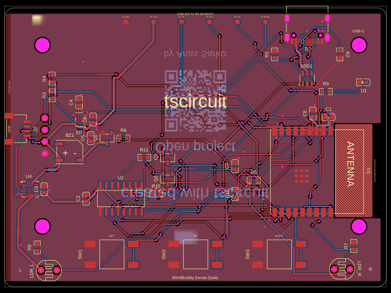 More from this authorAnasSarkiz/BlinkBuddyThis code defines and renders a 24mm square PCB silkscreen with a centered QR code graphic and labeling for open project instructions.
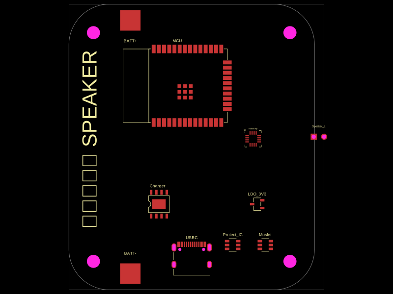 Similar packagemohan-bee/speakerThis code defines configurable 3D models and PCB footprints for various electronic components, including a battery charger IC, a dual Hall sensor, a dual power switch, and a voltage regulator, with detailed pinouts, footprints, and CAD models for schematic and physical design.
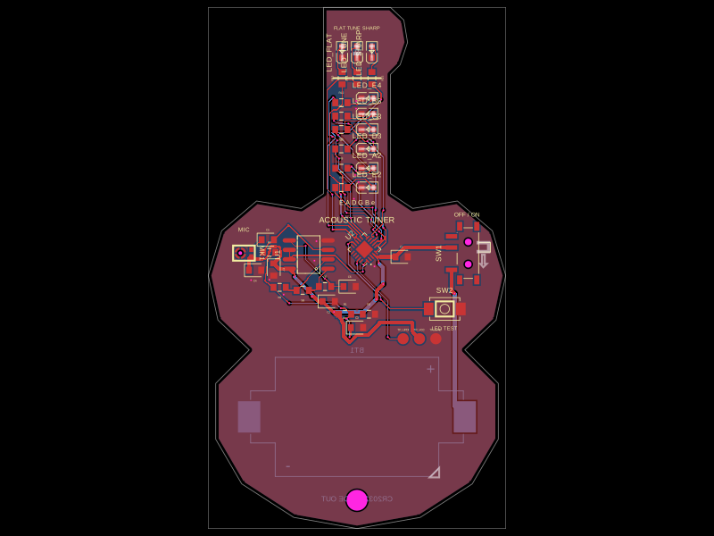 Discover something newgokul/acoustic-guitar-tunerThis code defines a miniature circuit board featuring a microcontroller (ATTINY1616-MNR), audio and power components, tactile switch, various LEDs, and passive components arranged with specific footprints, connections, and mechanical markings for a mini acoustic guitar tuner.