AnasSarkiz/ble-pedometer
This code defines and configures various electronic hardware components such as surface-mount resistors, crystals, diodes, transistors, connectors, and switches with their physical footprints, schematic symbols, and 3D CAD models for PCB assembly.
- Version
- 1.0.7
- License
- unset
- Stars
- 0
DESIGN_REVIEW.md
# Design review

The local 60 × 38 mm revision replaces BQ25150 with BQ25186DLHR and adds TPS7A0233DBVR. The user-approved package/power-tree redesign preserves 0.30 mm drill / 0.45 mm via pad minima. See [DRC_REPORT.md](DRC_REPORT.md) for actual routing checks, independent shorts and exporter blockers.

## Retained

- Four-layer, one-sided board with functional placement zones, three schematic sheets and eight sections.
- CC2340R5/BMA400 interrupt-driven sensing; BQ27427 in the actual battery current path.
- Power-only USB-C, battery NTC, wake button, charge/status control and SWD.
- OLED high-side power gating plus isolation of both bus lines.
- Edge antenna, copper keepout, fixed RF filter and optional tuning pads.

## Changed

- WSON charger with perimeter signal pads; independent always-on 3.3 V regulator.
- Separate VSYS_RAW and SYS_VDD rails. Exact supplier footprints and audited pin maps.
- Charge enable pulled high during MCU reset; old IMAX and TS-bias resistors removed. There is **no hardware IMAX ceiling** on the new charger. Firmware and pack qualification are mandatory.
- Nominal 4.7 µF input/battery capacitors provide derating margin; verify at least 1 µF effective capacitance across the operating range.
- Explicit MCU exposed-pad corner escape, with the connected decoupler ground still on GND.
- Authored through-via escapes for the accelerometer INT2 connection and the bridge between the MCU's VDDR pins. Wire segments are explicit on both sides of each via; regression tests verify continuous layer transitions and actual drill/pad sizes.
- Authored SWDIO and charger-enable routes, plus staggered native through-via nodes for the MCU supply, I²C and interrupt pins. These are real connected copper, not soft hints or artificial routing obstacles.

## Before fabrication release

1. Pass all routed geometry and independent-short checks; maintain the recorded via constraints.
2. Resolve full-stack drill-export conflicts and validate the exported files against canonical geometry.
3. Exclude DNP and bare test pads from assembly outputs; complete package/rotation metadata.
4. Qualify a protected pack, connector polarity, capacity, charging rate and 10 kΩ NTC curve.
5. Confirm OLED/harness pinout, rail minimum and timing.
6. Field-solve 50 Ω RF geometry for the actual stackup; qualify antenna performance in the final enclosure.
7. Obtain vendor CAM/stencil/assembly review, including remaining BQ27427 WLCSP and charger thermal-pad soldering.
8. Verify the cleaned-up silkscreen in exported CAM artwork: short references and text-envelope clearances now pass locally, but ink/stroke size, imported outlines, assembly identification and mask clearances still need vendor review.

## Electrical and mechanical verification

The keyed connector is not reverse-polarity protection. Use a controlled keyed/protected pack or implement protection before allowing arbitrary packs. The larger board requires new enclosure retention, plug/cable clearances, button access and antenna spacing.

Verify BQ27427 chemistry/capacity/termination parameters against the cell. Check I²C rise time with the actual harness: 4.7 kΩ and 75 pF gives approximately 299 ns, already near the 400 kHz limit. Qualify TPS7A02 dropout/load transients at low battery and suppress the display where needed.

Review the MCU decoupling loop inductance and ground/rail return paths against the TI layout guidance. Generic routed DRC and logical net connectivity do not prove adequate high-frequency decoupling; pin-to-net declarations also do not enforce every direct pin-to-capacitor distance automatically.

## First articles

Inspect bare-board continuity and soldering, including X-ray of U2/U3. Start with current-limited battery simulation, verify independent rails and CE-high, then program through SWD. Follow [CHARGER_BRINGUP.md](CHARGER_BRINGUP.md) before using a real pack. Exercise temperature faults, reset, USB handover, signed gauge current, step/tap interrupts, OLED isolation and sleep current. Complete RF/ESD/thermal and runtime measurements.

Neither a clean DRC nor these documents certify a production device. Firmware is not delivered or tested in this hardware revision.
Related Packages
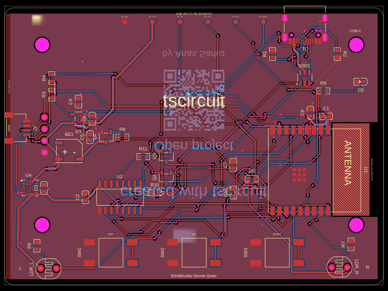 More from this authorAnasSarkiz/BlinkBuddyThis code defines and renders a 24mm square PCB silkscreen with a centered QR code graphic and labeling for open project instructions.
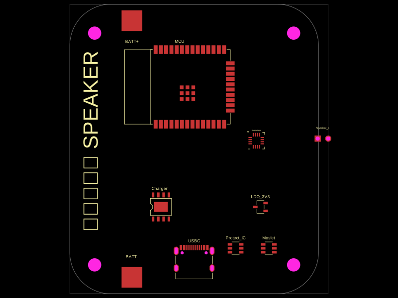 Similar packagemohan-bee/speakerThis code defines configurable 3D models and PCB footprints for various electronic components, including a battery charger IC, a dual Hall sensor, a dual power switch, and a voltage regulator, with detailed pinouts, footprints, and CAD models for schematic and physical design.
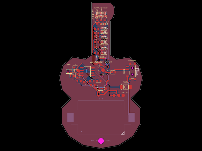 Discover something newgokul/acoustic-guitar-tunerThis code defines a miniature circuit board featuring a microcontroller (ATTINY1616-MNR), audio and power components, tactile switch, various LEDs, and passive components arranged with specific footprints, connections, and mechanical markings for a mini acoustic guitar tuner.