AnasSarkiz/ble-pedometer
This code defines and configures various electronic hardware components such as surface-mount resistors, crystals, diodes, transistors, connectors, and switches with their physical footprints, schematic symbols, and 3D CAD models for PCB assembly.
- Version
- 1.0.7
- License
- unset
- Stars
- 0
FABRICATION_NOTES.md
# Fabrication and assembly notes

## Construction

- 60 × 38 mm outline, nominal 1.0 mm thickness, four copper layers, one-sided assembly. Revise enclosure fit from the original 42 × 26 mm board.
- Intended stack: top components/signals, inner1 ground reference, inner2 power/slow signals, bottom signals/ground fill. Confirm actual routed ground-plane integrity and the vendor stackup.
- Minimum via drill **0.30 mm**, pad **0.45 mm**; blind/buried routing disabled.
- Green solder mask. Confirm the color in the manufacturer's order settings as well as the board source.
- Minimum trace 0.10 mm; trace-to-pad clearance 0.09 mm; via-to-pad and pad-to-pad clearance 0.10 mm; board-edge clearance 0.20 mm. No local HDI rule exemptions.
- Confirm copper, solder mask and dielectric thickness before RF impedance calculation.

## Charger package redesign

BQ25186DLHR, a WSON with perimeter signal pads and exposed thermal pad, replaces the blocked BQ25150 ball array. TPS7A0233DBVR supplies nominal 3.3 V independently. This removes the old charger escape constraint without reducing via sizes. The BQ27427 remains a 0.5 mm-pitch WLCSP.

Use exact imported DLH/YZF/DBV land patterns, not generic approximations. The charger still has 0.4 mm lead pitch. Stencil, thermal-pad paste, mask clearances, MSL/reflow and first-article X-ray require assembler review. A clean routed DRC is not assembly approval.

## Export blockers

The new `bun run export:manufacturing-review` workflow uses official Gerber exporter 0.0.104, which prioritizes physical via layers and deduplicates drill hits. Actual exported spans are checked: only L1–L4 plated drilling is accepted. The geometry gate retains full-stack physical layers and 0.30/0.45 mm minima; legacy routing transition endpoints are no longer mistaken for physical drill bounds. Do not edit generated Circuit JSON or resize vias after routing.

The official BOM 0.0.17 and PnP 0.0.13 exporters exclude DNP C23/C24 and bare TP1–TP6 without removing PCB copper. Exactly 50 fitted rows are verified in each output. A strict MPN/supplier resolver supplies the package descriptions documented in BOM.md.

**The old bundled `tsci export -f gerbers` command remains unsafe for this board.** Use only the new review workflow. The corrected output still needs supplier orientation/centroid sign-off: none of the 50 placements currently carries supplier pin-1 calibration. Existing source rotations are exported unchanged, not certified. This is missing verification, not evidence that all 50 rotations are wrong.

Old local Gerber archives are obsolete and must not be ordered. New files are explicitly marked review-only in their manifest; no manufacturing archive is released here. Vendor CAM review remains mandatory.

## RF

The antenna keepout and ground-pour notch move with the edge antenna. Inspect all copper layers, not only the top preview. The nominal 0.18 mm RF trace assumes approximately 0.10 mm top-to-reference dielectric; this is not a 50 Ω guarantee. Field-solve for the actual fabricator stackup and review discontinuities/return paths.

Retain the fixed filter order; populate R16 = 0 Ω and leave C23/C24 DNP initially. Tune with the final enclosure, battery, display cable, strap and plastics.

## Assembly and electrical checks

- Verify USB-C shell soldering and duplicated VBUS/GND contacts. Check CC1/CC2 each measure 5.1 kΩ to ground. Confirm socket/enclosure access against the [GCT drawing](https://gct.co/files/drawings/usb4105.pdf).
- J2/J3 are top-entry BM-series JST-SH headers. Allow vertical insertion/extraction clearance per the [JST catalog](https://www.jst-mfg.com/product/pdf/eng/eSH.pdf).
- Check battery polarity against the purchased pack. Connector keying is not electrical reverse-polarity protection.
- Qualify the protected cell, charging current and 10 kΩ NTC curve. There is no hardware IMAX resistor on BQ25186. Follow [CHARGER_BRINGUP.md](CHARGER_BRINGUP.md).
- Verify C1/C3 effective capacitance under bias/temperature and LDO input/output stability and dropout.
- Inspect fine-pitch bridges and display-off leakage; verify harness pinout before attaching a panel.
- Keep SWDIO, SWDCK, RESET, GND, SYS_VDD and charge-status pads exposed.
- Compact, individually placed references now pass the text-envelope clearance check. Confirm exported ink/stroke dimensions, imported footprint outlines, pin-one marks and solder-mask openings in vendor CAM review; this is not assembly artwork sign-off.
- Complete continuity, controlled power-up, charging-fault, RF, ESD and thermal testing before production approval.
Related Packages
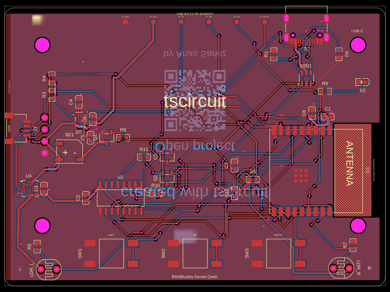 More from this authorAnasSarkiz/BlinkBuddyThis code defines and renders a 24mm square PCB silkscreen with a centered QR code graphic and labeling for open project instructions.
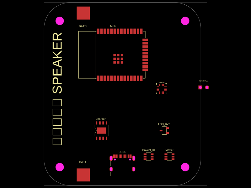 Similar packagemohan-bee/speakerThis code defines configurable 3D models and PCB footprints for various electronic components, including a battery charger IC, a dual Hall sensor, a dual power switch, and a voltage regulator, with detailed pinouts, footprints, and CAD models for schematic and physical design.
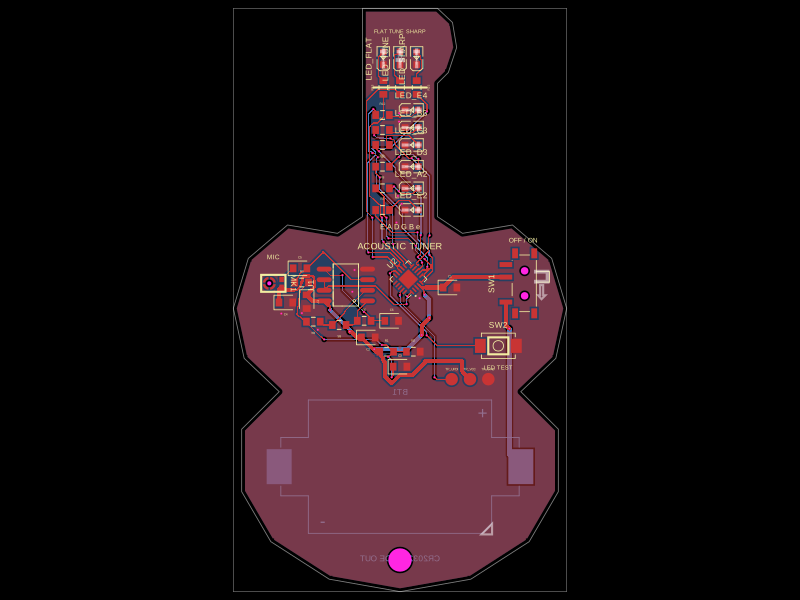 Discover something newgokul/acoustic-guitar-tunerThis code defines a miniature circuit board featuring a microcontroller (ATTINY1616-MNR), audio and power components, tactile switch, various LEDs, and passive components arranged with specific footprints, connections, and mechanical markings for a mini acoustic guitar tuner.