AnasSarkiz/ble-pedometer
This code defines and configures various electronic hardware components such as surface-mount resistors, crystals, diodes, transistors, connectors, and switches with their physical footprints, schematic symbols, and 3D CAD models for PCB assembly.
- Version
- 1.0.7
- License
- unset
- Stars
- 0
FANOUT_REVIEW.md
# Native fanout evaluation — 2026-09-05

Historical experiment: these results predate the user-approved BQ25186 WSON charger and TPS7A02 regulator redesign. Current validation is in [DRC_REPORT.md](DRC_REPORT.md); the failed BQ25150 trial below is not the current board.

**The original automatic fanout experiments below did not obtain a complete escape. Their settings were removed. The subsequent authored-escape work is described in the next section; current measured results are in DRC_REPORT.md. Nothing was committed or pushed.**

## Subsequent WSON revision and authored escapes

The user approved replacing the blocked BQ25150 with the BQ25186 WSON charger and an independent TPS7A02 regulator. This removes the original charger ball-array constraint without reducing the via dimensions. The BQ27427 gauge remains a WLCSP, rotated 180° with its BIN resistor moved to match the new escape direction.

Three attempted authored gauge-ground variants were rejected by the native topology-merging solver for inter-group overlap. They were removed, not counted as successful builds. The retained gauge uses ordinary native routing. Soft MCU trace hints also did not constrain the merged shared nets in the solver input and were removed.

The retained MCU strategy uses real native through-via nodes for VDDS1, I²C and interrupt signals, with staggered positions where the 0.5 mm pin pitch cannot accommodate a straight row of 0.45 mm via pads. Native `<trace pcbPath>` routes provide the exposed-pad ground escape, VDDR bridge, both SWD signals, charger-enable, SDA pull-up and accelerometer INT2 connections. The VDDD capacitor, crystal pair and RF-input connection have authored top-layer paths. The charger uses staggered native SYS, BAT, CE, PG and interrupt escape vias. No generated geometry, dependencies, obstacle set or DRC filters were patched.

The built-in `beta-pipeline9` preloaded-trace mode was also tested after confirming its implementation and invalidating the exact stale Pipeline7 route cache (preserved under `dist/route31-pipeline7-cache.json`). It failed its high-density routing validator on a ground connection and returned only authored traces. That failed output was rejected, and the retained design uses `auto_local` again. No alternate solver was silently installed or substituted.

The native via bottom port is exposed to the remaining routed net, while the authored top copper reaches the same physical through via. Regression tests check net identity, escape positions, continuity, and actual 0.30/0.45 mm dimensions. Both sides of each inline via have explicit wire endpoints. Board `pcbStyle` sets those inline-via sizes in addition to the unchanged board minimum rules.

The final native board-routing phase uses extra planning margin (0.16 mm trace/pad, 0.22 mm via/pad and 0.30 mm hole-edge spacing). The original acceptance rules remain 0.09 mm trace/pad, 0.10 mm via/pad and the specified drill minima. The actual phase input was inspected to verify these settings reach the solver. Full-board DRC and the independent short check remain separate from source-only regression tests.

Final validation reached **0 DRC errors and 0 independent shorts**, with 166 traces and 119 vias at the requested minima. Native shared via nodes replace the inline VDDR bridge endpoints; additional charger SDA and TS/MR escapes and an MCU VDDS2 escape complete the retained strategy. Sixty-nine drill-export conflicts still block fabrication. See DRC_REPORT.md for the exact final artifact, all warnings, and verification scope.

## Historical automatic fanout experiment

Used the tscircuit skill, the current official handbook, pinned tscircuit 0.0.2463 and the installed `@tscircuit/fanout-solver` 0.0.46. Native `autoroutingphase` with `autorouter="fanout"` runs the dedicated fanout solver before its downstream board router; it is not the same as ordinary board autorouting. No dependency code or generated geometry was patched.

## Tests and scope

Every experiment retained the board's 0.30 mm minimum drill, 0.45 mm minimum via pad, 0.10 mm trace width minimum, 0.09 mm trace-to-pad clearance, 0.10 mm via-to-pad clearance and prohibition on blind/buried vias. All four copper layers were offered to the fanout solver. Via-in-pad was not enabled. Existing physical copper pours were retained, with the fanout phase explicitly selecting `inner1` for ground termination.

| Target | Boundary padding | Best completed escapes / selected connections | Remaining escape failures |
|---|---:|---:|---|
| U2 BQ25150 charger | 1 mm | 2 / 4 | CE (C2), IMAX (C3) |
| U2 BQ25150 charger | 3 mm | 2 / 4 | No improvement in completion; same constrained inner-pad geometry |
| U1 CC2340 MCU | 1 mm | 6 / 7 | Exposed-pad ground |
| U3 BQ27427 gauge | 1 mm | 3 / 4 | Center VSS2 (B2) ground |

These are **partial diagnostic connection counts, not package pin counts, full-board routing percentages or DRC passes**. All pin selectors were supplied for each target. The installed phase filtering selected only its direct trace connections and source-only ground terminations; merged multi-endpoint signal/power nets were not included in these fanout inputs. This coverage limitation must also be resolved before adopting per-package fanout. Every selected problem already failed, so none proceeded to a validated downstream routed board.

The native `<breakout>` alternative was also attempted around the charger. In this project's imported-footprint setup, rendering failed in `doInitialCreateAutoplacedBreakoutPoints`: it tried to resolve `.D1_VBUS_TVS > .C` before that component had ports. This is an integration failure, not evidence that the electrical connection is absent. Removing the experimental wrapper restored the passing source and placement tests. No workaround or dependency patch was installed.

The fanout plane choice must be supplied directly to the routing phase in this pinned version. Adding it only at board level did not prevent the automatic inference from finding ground on multiple layers and aborting before the solver. The successful solver-starting tests used `fanoutPourNetMap={{ inner1: "GND" }}` on `autoroutingphase`.

## Why more board area did not solve the charger escape

The actual imported charger footprint has approximately 0.40005 mm ball pitch and 0.20 mm pad diameter, leaving approximately 0.20 mm between adjacent pad edges. A minimum 0.10 mm trace with 0.09 mm clearance to both neighboring pads requires 0.28 mm. Ordinary escape through that gap cannot satisfy the current rule.

A centered interstitial 0.45 mm via pad is also too large: its center would be about 0.283 mm from the four surrounding pad centers, while a foreign pad requires approximately 0.425 mm (0.100 mm ball-pad radius + 0.225 mm via-pad radius + 0.100 mm clearance). Increasing the outer breakout boundary does not enlarge these local gaps. This geometric check and the failed inner-pad escapes support a package/rule incompatibility for conventional fanout; they are not a claim that every possible manufacturing technology has been tested.

The MCU and gauge failures are specifically ground escapes. They need an intentional, assembly-reviewed ground-via strategy, including solder-wicking/thermal-pad implications if via-in-pad is chosen. Their failed default fanout attempts do not establish that the parts are intrinsically unroutable.

## Evidence and reproduction

Local, ignored diagnostic artifacts are under:

- `dist/fanout-charger/` and `dist/fanout-charger-3mm/`
- `dist/fanout-mcu/`
- `dist/fanout-gauge/`

Each contains the solver's actual input, a phase error record, an unrouted PCB preview and constructor-input diagnostics under `solvers/index/solver-inputs.json`. Corresponding build logs are `dist/fanout-*-build.log`. Best-attempt failure identities were checked by replaying the recorded solver inputs. Partial solver plans were not exported into the board.

For the charger experiment, insert this native directive directly inside the board temporarily, keeping every existing board constraint:

```tsx
<autoroutingphase
  name="charger_fanout"
  phaseIndex={0}
  autorouter="fanout"
  fanoutBoundaryPadding="1mm"
  fanoutRoutingLayers={["top", "inner1", "inner2", "bottom"]}
  fanoutPourNetMap={{ inner1: "GND" }}
  connections={[
    "IN", "PMID1", "BAT1", "GND", "PG", "PMID2", "BAT2", "TS",
    "MR", "CE", "IMAX", "ADCIN", "VDD", "INT", "LP", "LSLDO",
    "VIO", "SDA", "SCL", "VINLS",
  ].map((pin) => `.U2_CHARGER > .${pin}`)}
/>
```

Run source/placement checks first, then the diagnostic build:

```sh
bun run check:review
bunx tsci build index.circuit.tsx --autorouter-timeout 300s --autorouter-debug --autorouter-debug-dir dist/fanout-charger --autorouter-dump-srj all --solver-debug --solver-debug-dir dist/fanout-charger/solvers --pcb-png
```

The CLI returned zero despite printing an asynchronous fanout error and emitting an unrouted circuit. Its exit status is not a fabrication pass. The separate fabrication gate rejects missing routing. Do not substitute the failed experiment's output for the retained routed-board result or count its missing routes as a DRC improvement.

## Decision

Do not enable this failed configuration in the review design. Preserve the current clearances, via limits, components, placements, three schematic sheets and eight sections. The previous routed baseline remains 21 emitted DRC records, one independently detected short and 97 drill-span conflicts; see `DRC_REPORT.md` for the distinct gates.

After removing the experimental directives, the retained source was rebuilt and verified: 11 tests and four snapshots pass, netlist and placement checks report no issues, all compiled source trace definitions match the pre-fanout baseline, and routing again emits 158 traces, 21 DRC records, 24 warnings and 140 vias at 0.30/0.45 mm. The independent short check still exits 1 and the fabrication gate still reports 118 blockers. The failed gauge output is separately retained under `dist/fanout-gauge/failed-circuit.json`; the gate rejects it for missing routing and emitted errors, rather than accepting the CLI's zero exit status.

To proceed toward production while retaining the via limits, review a larger-pitch charger/power-path replacement and its electrical consequences. Separately resolve native fanout coverage/integration and the MCU/gauge ground-via strategy, then rerun full routing, DRC, connectivity and drill-export checks. Changing charger architecture or adopting a different fabrication process requires the user's decision, not an automatic substitution.

References: [tscircuit handbook](https://github.com/tscircuit/handbook), [fanout solver](https://github.com/tscircuit/fanout-solver), [native prop definitions](https://github.com/tscircuit/props). Installed source/types and recorded solver inputs were used to verify behavior of the pinned build.
Related Packages
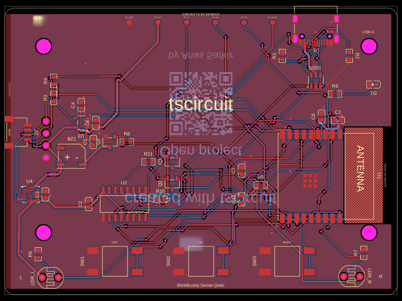 More from this authorAnasSarkiz/BlinkBuddyThis code defines and renders a 24mm square PCB silkscreen with a centered QR code graphic and labeling for open project instructions.
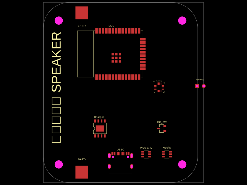 Similar packagemohan-bee/speakerThis code defines configurable 3D models and PCB footprints for various electronic components, including a battery charger IC, a dual Hall sensor, a dual power switch, and a voltage regulator, with detailed pinouts, footprints, and CAD models for schematic and physical design.
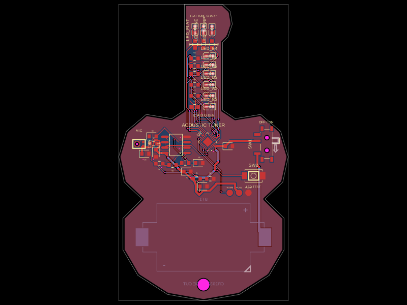 Discover something newgokul/acoustic-guitar-tunerThis code defines a miniature circuit board featuring a microcontroller (ATTINY1616-MNR), audio and power components, tactile switch, various LEDs, and passive components arranged with specific footprints, connections, and mechanical markings for a mini acoustic guitar tuner.