AnasSarkiz/ble-pedometer
This code defines and configures various electronic hardware components such as surface-mount resistors, crystals, diodes, transistors, connectors, and switches with their physical footprints, schematic symbols, and 3D CAD models for PCB assembly.
- Version
- 1.0.7
- License
- unset
- Stars
- 0
PINMAP.md
# Pin map

## CC2340R52E0RGER allocation

| MCU signal | Board net | Function / boot expectation |
|---|---|---|
| DIO24/A7 | I2C_SCL | 400 kHz shared internal I²C clock |
| DIO12 | I2C_SDA | Shared internal I²C data |
| DIO8 | ACCEL_INT1 | BMA400 step/activity wake |
| DIO11 | ACCEL_INT2 | BMA400 double-tap wake |
| DIO20/A11 | GAUGE_INT_N | BQ27427 open-drain GPOUT |
| DIO21/A10 | CHG_INT_N | BQ25186 open-drain interrupt |
| DIO6/A1 | CHG_PG_N | BQ25186 open-drain power-good |
| DIO3/X32P | CHG_CE_N | High at reset through 100 kΩ; keep high until charge configuration is read back, then drive low |
| DIO13 | DISP_PWR_N | Active-low P-MOS gate; default high from 100 kΩ pull-up |
| DIO4/X32N | DISP_BUS_EN | Enables both I²C analog switches; default low from 100 kΩ pull-down |
| DIO16/SWDIO | SWDIO | Programming/debug pad TP1 |
| DIO17/SWDCK | SWDCK | Programming/debug pad TP2 |
| RSTN | RESET_N | 100 kΩ pull-up, 100 nF to GND, TP3 |
| X48P / X48N | — | 48 MHz crystal pins |
| ANT | RF_FILTER_IN | RF output into matching/filter network |
| DCDC | — | 10 µH to VDDR |
| VDDR1/VDDR2 | VDDR | 10 µF plus two 100 nF local bypass capacitors |
| VDDD | — | 1 µF local decoupling only |
| VDDS1/2/3 | SYS_VDD | 3.3 V rail, three 100 nF plus 10 µF bulk |
| GND/EP | GND | Solid ground connection and exposed-pad thermal vias/copper |

Unused GPIOs remain uncommitted in this revision and should be left in their reset state unless firmware deliberately assigns them.

## Connectors

### J1 USB-C (USB4105-GF-A)

| Contacts | Connection |
|---|---|
| A4, A9, B4, B9 | VBUS |
| A1, A12, B1, B12, shell | GND |
| A5 / CC1 | 5.1 kΩ to GND |
| B5 / CC2 | 5.1 kΩ to GND |
| A6/A7/B6/B7, SBU1/SBU2 | No connect; power-only port |

### J2 battery (JST-SH 3 pin)

| Pin | Signal |
|---|---|
| 1 | BATTERY_POS / BAT_CELL |
| 2 | BATT_NTC; intended 10 kΩ NTC in qualified pack |
| 3 | GND |

Never attach a two-wire pack to this footprint without a qualified NTC adapter or an explicitly reviewed TS network.

### J3 display (JST-SH 4 pin)

| Pin | Signal |
|---|---|
| 1 | DISP_VDD, switched 3.3 V |
| 2 | GND |
| 3 | DISP_SDA, isolated while off |
| 4 | DISP_SCL, isolated while off |

The harness must be verified against the chosen display module; small OLED boards do not use a universal four-pin ordering.
Related Packages
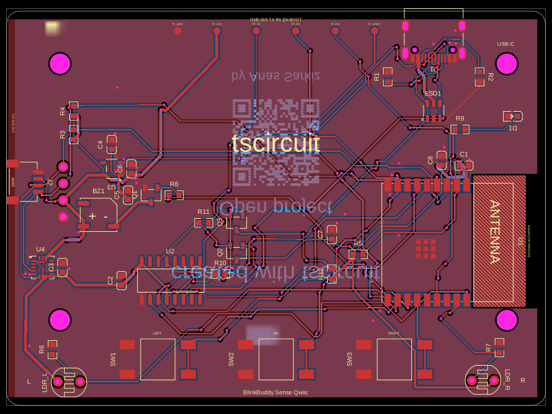 More from this authorAnasSarkiz/BlinkBuddyThis code defines and renders a 24mm square PCB silkscreen with a centered QR code graphic and labeling for open project instructions.
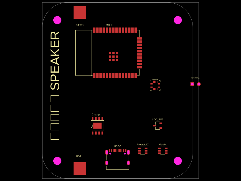 Similar packagemohan-bee/speakerThis code defines configurable 3D models and PCB footprints for various electronic components, including a battery charger IC, a dual Hall sensor, a dual power switch, and a voltage regulator, with detailed pinouts, footprints, and CAD models for schematic and physical design.
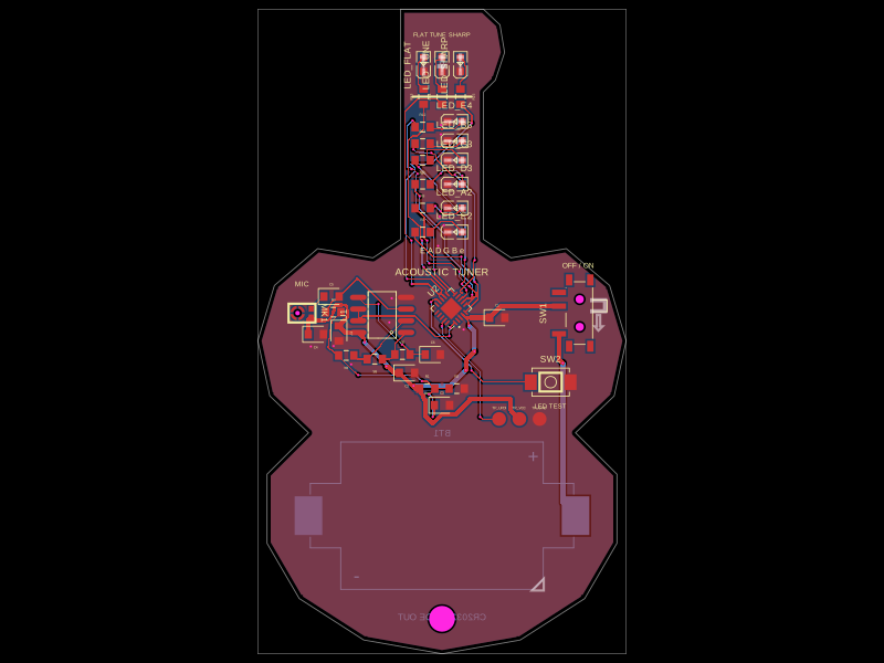 Discover something newgokul/acoustic-guitar-tunerThis code defines a miniature circuit board featuring a microcontroller (ATTINY1616-MNR), audio and power components, tactile switch, various LEDs, and passive components arranged with specific footprints, connections, and mechanical markings for a mini acoustic guitar tuner.