AnasSarkiz/ble-pedometer
This code defines and configures various electronic hardware components such as surface-mount resistors, crystals, diodes, transistors, connectors, and switches with their physical footprints, schematic symbols, and 3D CAD models for PCB assembly.
- Version
- 1.0.7
- License
- unset
- Stars
- 0
imports/USB4105_GF_A.tsx
import type { ChipProps } from "@tscircuit/props"

const pinLabels = {
  pin1: ["EH"],
  pin2: ["pin2"],
  pin3: ["pin3"],
  pin4: ["pin4"],
  pin5: ["A12","GND1"],
  pin6: ["B1","GND2"],
  pin7: ["A9","VBUS1"],
  pin8: ["B4","VBUS2"],
  pin9: ["B5","CC2"],
  pin10: ["A8","SBU1"],
  pin11: ["B6","DP2"],
  pin12: ["A7","DN1"],
  pin13: ["A6","DP1"],
  pin14: ["B7","DN2"],
  pin15: ["A5","CC1"],
  pin16: ["B8","SBU2"],
  pin17: ["B9","VBUS3"],
  pin18: ["A4","VBUS4"],
  pin19: ["B12","GND3"],
  pin20: ["A1","GND4"]
} as const

const pinAttributes = {
  pin5: { requiresGround: true },
  pin6: { requiresGround: true },
  pin10: { doNotConnect: true },
  pin11: { doNotConnect: true },
  pin12: { doNotConnect: true },
  pin13: { doNotConnect: true },
  pin14: { doNotConnect: true },
  pin16: { doNotConnect: true },
  pin19: { requiresGround: true },
  pin20: { requiresGround: true },
} as const

export const USB4105_GF_A = (props: ChipProps<typeof pinLabels>) => {
  return (
    <chip
      pinLabels={pinLabels}
      pinAttributes={pinAttributes}
      supplierPartNumbers={{
  "jlcpcb": [
    "C3020560"
  ]
}}
      manufacturerPartNumber="USB4105-GF-A"
      footprint={<footprint insertionDirection="from_bottom">
        <hole pcbX="2.890012mm" pcbY="1.0646474mm" diameter="0.649986mm" />
<hole pcbX="-2.890012mm" pcbY="1.0646474mm" diameter="0.649986mm" />
<platedhole  portHints={["pin1"]} pcbX="-4.320032mm" pcbY="1.5444534mm" holeWidth="0.700024mm" holeHeight="1.700022mm" outerWidth="1.0999978mm" outerHeight="2.0999958mm" shape="pill" />
<platedhole  portHints={["pin2"]} pcbX="4.320032mm" pcbY="1.5444534mm" holeWidth="0.700024mm" holeHeight="1.700022mm" outerWidth="1.0999978mm" outerHeight="2.0999958mm" shape="pill" />
<platedhole  portHints={["pin3"]} pcbX="4.320032mm" pcbY="-2.6356246mm" holeWidth="0.700024mm" holeHeight="1.4000226mm" outerWidth="1.0999978mm" outerHeight="1.7999964mm" shape="pill" />
<platedhole  portHints={["pin4"]} pcbX="-4.320032mm" pcbY="-2.6356246mm" holeWidth="0.700024mm" holeHeight="1.4000226mm" outerWidth="1.0999978mm" outerHeight="1.7999964mm" shape="pill" />
<smtpad portHints={["pin5"]} pcbX="3.350006mm" pcbY="2.1096034mm" width="0.2999994mm" height="1.1500104mm" shape="rect" />
<smtpad portHints={["pin6"]} pcbX="3.050032mm" pcbY="2.1096034mm" width="0.2999994mm" height="1.1500104mm" shape="rect" />
<smtpad portHints={["pin7"]} pcbX="2.549906mm" pcbY="2.1098574mm" width="0.2999994mm" height="1.1500104mm" shape="rect" />
<smtpad portHints={["pin8"]} pcbX="2.249932mm" pcbY="2.1098574mm" width="0.2999994mm" height="1.1500104mm" shape="rect" />
<smtpad portHints={["pin9"]} pcbX="1.75006mm" pcbY="2.1096034mm" width="0.2999994mm" height="1.1500104mm" shape="rect" />
<smtpad portHints={["pin10"]} pcbX="1.24968mm" pcbY="2.1106194mm" width="0.2999994mm" height="1.1500104mm" shape="rect" />
<smtpad portHints={["pin11"]} pcbX="0.750062mm" pcbY="2.1096034mm" width="0.2999994mm" height="1.1500104mm" shape="rect" />
<smtpad portHints={["pin12"]} pcbX="0.249936mm" pcbY="2.1096034mm" width="0.2999994mm" height="1.1500104mm" shape="rect" />
<smtpad portHints={["pin13"]} pcbX="-0.249936mm" pcbY="2.1096034mm" width="0.2999994mm" height="1.1500104mm" shape="rect" />
<smtpad portHints={["pin14"]} pcbX="-0.750062mm" pcbY="2.1096034mm" width="0.2999994mm" height="1.1500104mm" shape="rect" />
<smtpad portHints={["pin15"]} pcbX="-1.249934mm" pcbY="2.1096034mm" width="0.2999994mm" height="1.1500104mm" shape="rect" />
<smtpad portHints={["pin16"]} pcbX="-1.75006mm" pcbY="2.1106194mm" width="0.2999994mm" height="1.1500104mm" shape="rect" />
<smtpad portHints={["pin17"]} pcbX="-2.249932mm" pcbY="2.1096034mm" width="0.2999994mm" height="1.1500104mm" shape="rect" />
<smtpad portHints={["pin18"]} pcbX="-2.549906mm" pcbY="2.1096034mm" width="0.2999994mm" height="1.1500104mm" shape="rect" />
<smtpad portHints={["pin19"]} pcbX="-3.050032mm" pcbY="2.1096034mm" width="0.2999994mm" height="1.1500104mm" shape="rect" />
<smtpad portHints={["pin20"]} pcbX="-3.350006mm" pcbY="2.1096034mm" width="0.2999994mm" height="1.1500104mm" shape="rect" />
<silkscreenpath route={[{"x":4.4699935999999525,"y":-1.5190659999998388},{"x":4.4699935999999525,"y":0.2778824000001805}]} />
<silkscreenpath route={[{"x":-4.469993600000066,"y":-3.7522085999999035},{"x":-4.469993600000066,"y":-5.254948799999966},{"x":4.4699935999999525,"y":-5.254948799999966},{"x":4.4699935999999525,"y":-3.7522085999999035}]} />
<silkscreenpath route={[{"x":-4.469993600000066,"y":0.2778824000001805},{"x":-4.469993600000066,"y":-1.5190659999998388}]} />
<silkscreentext text="{NAME}" pcbX="-0.018288mm" pcbY="3.6902474mm" anchorAlignment="center" fontSize="1mm" />
<courtyardoutline outline={[{"x":-5.132387999999992,"y":2.9402474000000893},{"x":5.0958120000000235,"y":2.9402474000000893},{"x":5.0958120000000235,"y":-5.509952599999906},{"x":-5.132387999999992,"y":-5.509952599999906},{"x":-5.132387999999992,"y":2.9402474000000893}]} />
      </footprint>}
      cadModel={{
        objUrl: "https://modelcdn.tscircuit.com/easyeda_models/assets/C3020560.obj?uuid=b568c80088e44e7787ac98e18b16aaa3",
        stepUrl: "https://modelcdn.tscircuit.com/easyeda_models/assets/C3020560.step?uuid=b568c80088e44e7787ac98e18b16aaa3",
        pcbRotationOffset: 0,
        modelOriginPosition: { x: 0, y: 1.5075092000000494, z: -0.0000020000000000575113 },
      }}
      {...props}
    />
  )
}
Related Packages
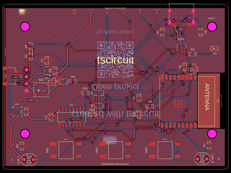 More from this authorAnasSarkiz/BlinkBuddyThis code defines and renders a 24mm square PCB silkscreen with a centered QR code graphic and labeling for open project instructions.
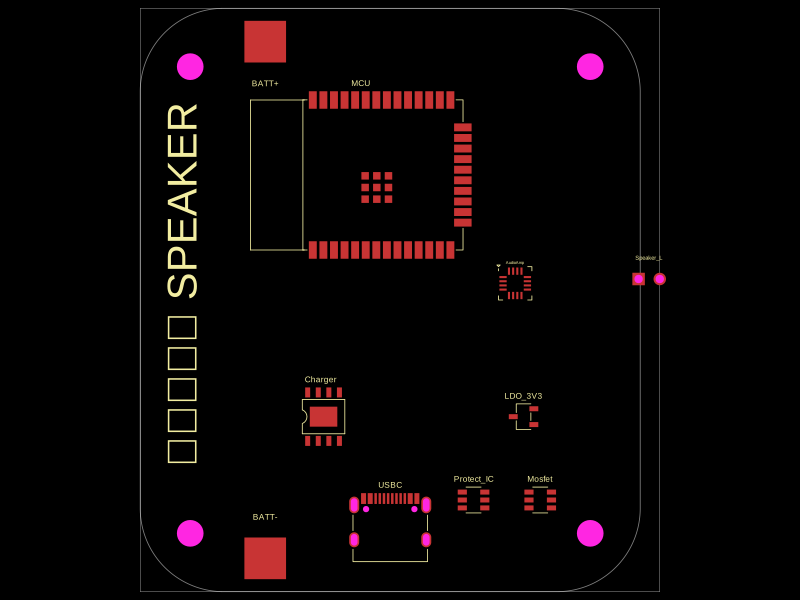 Similar packagemohan-bee/speakerThis code defines configurable 3D models and PCB footprints for various electronic components, including a battery charger IC, a dual Hall sensor, a dual power switch, and a voltage regulator, with detailed pinouts, footprints, and CAD models for schematic and physical design.
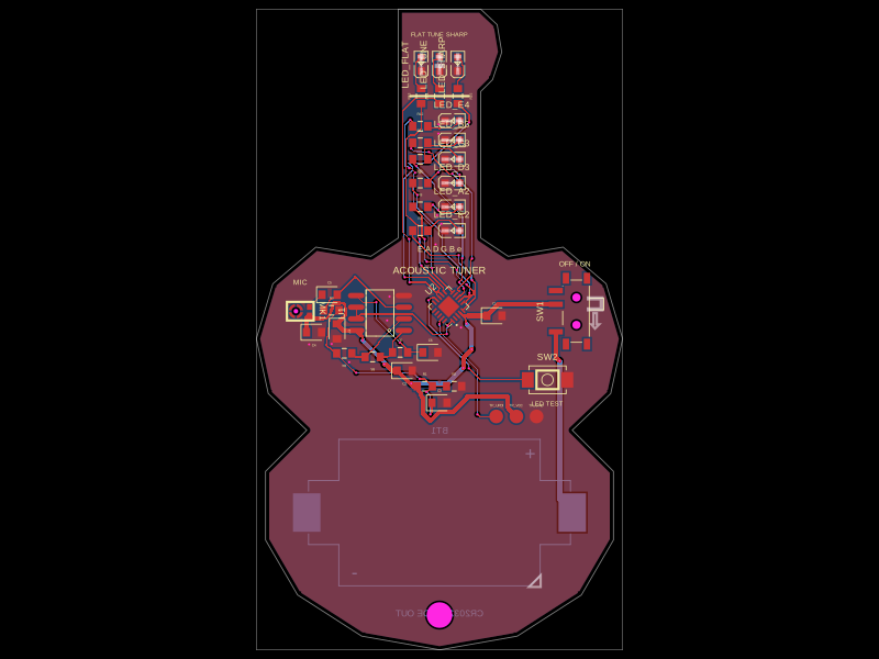 Discover something newgokul/acoustic-guitar-tunerThis code defines a miniature circuit board featuring a microcontroller (ATTINY1616-MNR), audio and power components, tactile switch, various LEDs, and passive components arranged with specific footprints, connections, and mechanical markings for a mini acoustic guitar tuner.