ShiboSoftwareDev/mspm0g3507-usb-c-dev-board
The circuit assembles a USB-C port with integrated ESD protection, power regulation, UART interface, and microcontroller (MSPM0G3507) with supporting components for USB data lines, CC termination, I2C, SPI, reset circuitry, and indicator LEDs.
- Version
- 1.4.2
- License
- unset
- Stars
- 0
index.circuit.tsx
PCB
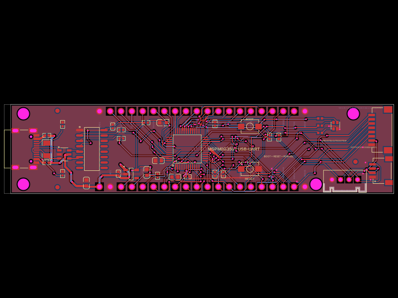
Schematic

import { AP2112K_3_3TRG1 } from "./imports/AP2112K_3_3TRG1"
import { A_0402WGF0000TCE } from "./imports/A_0402WGF0000TCE"
import { A_0402WGF1001TCE } from "./imports/A_0402WGF1001TCE"
import { A_0402WGF1002TCE } from "./imports/A_0402WGF1002TCE"
import { A_0402WGF3300TCE } from "./imports/A_0402WGF3300TCE"
import { A_0402WGF4701TCE } from "./imports/A_0402WGF4701TCE"
import { A_0402WGF4702TCE } from "./imports/A_0402WGF4702TCE"
import { A_0402WGF5101TCE } from "./imports/A_0402WGF5101TCE"
import { A_1206W4F0000T5E } from "./imports/A_1206W4F0000T5E"
import { CH340C } from "./imports/CH340C"
import { CL05B103KB5NNNC } from "./imports/CL05B103KB5NNNC"
import { CL05B104KO5NNNC } from "./imports/CL05B104KO5NNNC"
import { CL10A106KP8NNNC } from "./imports/CL10A106KP8NNNC"
import { CL10A475KO8NNNC } from "./imports/CL10A475KO8NNNC"
import { CL10B474KA8NNNC } from "./imports/CL10B474KA8NNNC"
import { MSPM0G3507SPTR } from "./imports/MSPM0G3507SPTR"
import { SM04B_SRSS_TB_LF__SN_ } from "./imports/SM04B_SRSS_TB_LF__SN_"
import { SM08B_SRSS_TB_LF__SN_ } from "./imports/SM08B_SRSS_TB_LF__SN_"
import { SZYY1615RGB_A_4pin } from "./imports/SZYY1615RGB_A_4pin"
import { TS342A2P_WZ } from "./imports/TS342A2P_WZ"
import { TYPE_C_31_M_12 } from "./imports/TYPE_C_31_M_12"
import { USBLC6_2SC6 } from "./imports/USBLC6_2SC6"
import { XL_1608SYGC_06 } from "./imports/XL_1608SYGC_06"
import { ZX_HY2_0_4PZZ } from "./imports/ZX_HY2_0_4PZZ"

const jlc = (partNumber: string) => ({ jlcpcb: [partNumber] })
const cleanComponentSilk = {
  pcbSx: { "& silkscreentext": { visibility: "hidden" as const } },
}

const MAIN_SCHEMATIC_SHEET = "MAIN"
const schematicSections = {
  usbConnector: "USB_CONNECTOR",
  usbUart: "USB_UART",
  power: "POWER",
  mcu: "MCU_CONTROL",
  rgb: "RGB_DEBUG",
  i2c: "I2C",
  spi: "SPI",
  headers: "HEADERS",
} as const

const schematicSectionStyle = (schSectionName: string) => ({
  ...cleanComponentSilk,
  schSectionName,
})

const HeaderPad = ({ index }: { index: number }) => (
  <platedhole
    name={`HEADER_PAD_${index + 1}`}
    portHints={[`pin${index + 1}`]}
    pcbX={`${(index - 9.5) * 2.54}mm`}
    pcbY="0mm"
    shape="circular_hole_with_rect_pad"
    holeDiameter="1.05mm"
    rectPadWidth="1.6mm"
    rectPadHeight="1.6mm"
    rectBorderRadius="0.8mm"
  />
)

const headerFootprint = (
  <footprint>
    {Array.from({ length: 20 }, (_, index) => (
      <HeaderPad key={`header-pad-${index + 1}`} index={index} />
    ))}
    <courtyardrect width="50.56mm" height="2.3mm" />
  </footprint>
)

const topHeaderPins = [
  "GND", "PA27", "PA26", "PA25", "PA24", "PA23", "PA22", "PA21",
  "PA20_SWCLK", "PA19_SWDIO", "PA18_BSL_INVOKE", "PA17", "PA16",
  "PA15", "PA14", "PA13", "PA12", "MCU_RESET_N", "VDD_3V3", "GND",
] as const

const bottomHeaderPins = [
  "VBUS_5V", "GND", "VDD_3V3", "PA0_I2C_SDA", "PA1_I2C_SCL",
  "PA2", "PA3", "PA4", "PA5", "PA6", "PA7", "PA8_SPI_DC",
  "PA9_SPI_RST", "PA10_UART_TX", "PA11_UART_RX", "PB6_SPI_CS",
  "PB7_SPI_MISO", "PB8_SPI_MOSI", "PB9_SPI_SCK", "GND",
] as const

const topSilkLabels = [
  "1 GND", "2 PA27", "3 PA26", "4 PA25", "5 PA24", "6 PA23",
  "7 PA22", "8 PA21", "9 SWCLK", "10 SWDIO", "11 BOOT/PA18",
  "12 PA17", "13 PA16", "14 PA15", "15 PA14", "16 PA13", "17 PA12",
  "18 RESET", "19 3V3", "20 GND",
] as const

const bottomSilkLabels = [
  "1 VBUS", "2 GND", "3 3V3", "4 SDA/PA0", "5 SCL/PA1", "6 PA2",
  "7 PA3", "8 PA4", "9 PA5", "10 PA6", "11 PA7", "12 DC/PA8",
  "13 RST/PA9", "14 TX/PA10", "15 RX/PA11", "16 CS/PB6",
  "17 MISO/PB7", "18 MOSI/PB8", "19 SCK/PB9", "20 GND",
] as const

const mcuBreakoutNets = [
  ["PA0", "PA0_I2C_SDA"], ["PA1", "PA1_I2C_SCL"], ["PA2", "PA2"],
  ["PA3", "PA3"], ["PA4", "PA4"], ["PA5", "PA5"], ["PA6", "PA6"],
  ["PA7", "PA7"], ["PA8", "PA8_SPI_DC"], ["PA9", "PA9_SPI_RST"],
  ["PA10", "PA10_UART_TX"], ["PA11", "PA11_UART_RX"],
  ["PB2", "PB2_RGB_RED"], ["PB3", "PB3_RGB_GREEN"],
  ["PB6", "PB6_SPI_CS"], ["PB7", "PB7_SPI_MISO"],
  ["PB8", "PB8_SPI_MOSI"], ["PB9", "PB9_SPI_SCK"],
  ["PB14", "PB14_RGB_BLUE"],
  ["PA12", "PA12"], ["PA13", "PA13"], ["PA14", "PA14"],
  ["PA15", "PA15"], ["PA16", "PA16"], ["PA17", "PA17"],
  ["PA18", "PA18_BSL_INVOKE"], ["PA19", "PA19_SWDIO"],
  ["PA20", "PA20_SWCLK"], ["PA21", "PA21"], ["PA22", "PA22"],
  ["PA23", "PA23"], ["PA24", "PA24"], ["PA25", "PA25"],
  ["PA26", "PA26"], ["PA27", "PA27"],
] as const

const headerNet = (label: string) => label === "GND" ? "net.GND" : `net.${label}`

const HeaderSilkLabel = ({ text, x, y }: { text: string, x: number, y: number }) => (
  <silkscreentext text={text} pcbX={x} pcbY={y} pcbRotation={90} fontSize="0.48mm" anchorAlignment="center" layer="bottom" />
)

const NamedTrace = ({ name, from, to }: { name: string, from: string, to: string }) => (
  <trace name={name} from={from} to={to} />
)

export default function MSPM0G3507UsbCDevBoard() {
  return (
    <board
      title="MSPM0G3507 USB-C Dev Board"
      outline={[
        { x: -45, y: 10.5 },
        { x: 45, y: 10.5 },
        { x: 45, y: -10.5 },
        { x: -45, y: -10.5 },
      ]}
      layers={2}
      schSheetName={MAIN_SCHEMATIC_SHEET}
      schY={10}
      schAutoLayoutEnabled
      minViaHoleDiameter="0.3mm"
      minViaPadDiameter="0.45mm"
      minViaEdgeToPadEdgeClearance="0.2mm"
    >
      <schematicsheet
        name={MAIN_SCHEMATIC_SHEET}
        displayName="MSPM0G3507 USB-C Development Board"
        sheetSize="ANSI_B"
        sheetWidth="431.8mm"
        sheetHeight="279.4mm"
      >
        <schematicsection name={schematicSections.usbConnector} displayName="USB-C receptacle & CC" sectionTitleFontSize="0.35mm" />
        <schematicsection name={schematicSections.usbUart} displayName="USB protection & UART bridge" sectionTitleFontSize="0.35mm" />
        <schematicsection name={schematicSections.power} displayName="5 V to 3.3 V power" sectionTitleFontSize="0.35mm" />
        <schematicsection name={schematicSections.mcu} displayName="MCU, reset & boot" sectionTitleFontSize="0.35mm" />
        <schematicsection name={schematicSections.rgb} displayName="RGB debug LED" sectionTitleFontSize="0.35mm" />
        <schematicsection name={schematicSections.i2c} displayName="I2C connectors" sectionTitleFontSize="0.35mm" />
        <schematicsection name={schematicSections.spi} displayName="SPI display connector" sectionTitleFontSize="0.35mm" />
        <schematicsection name={schematicSections.headers} displayName="GPIO & debug headers" sectionTitleFontSize="0.35mm" />
      </schematicsheet>

      <TYPE_C_31_M_12
        {...schematicSectionStyle(schematicSections.usbConnector)}
        name="J_USB_C"
        noConnect={["A8", "B8"]}
        obstructsWithinBounds={false}
        pcbX={-41.1}
        pcbY={0}
        pcbRotation={-90}
        schX={-12.78}
        schY={-4.45}
      />
      <A_1206W4F0000T5E {...schematicSectionStyle(schematicSections.usbConnector)} name="R_USB_DM_JOIN" pcbX={-36.5} pcbY={-0.1} pcbRotation={90} obstructsWithinBounds={false} schX={-14.65} schY={-6.69} />
      <A_0402WGF0000TCE {...schematicSectionStyle(schematicSections.usbConnector)} name="R_VBUS_A_LINK" pcbX={-36.5} pcbY={3.2} obstructsWithinBounds={false} />
      <A_0402WGF0000TCE {...schematicSectionStyle(schematicSections.usbConnector)} name="R_VBUS_B_LINK" pcbX={-36.5} pcbY={-3.2} obstructsWithinBounds={false} />
      <USBLC6_2SC6 {...schematicSectionStyle(schematicSections.usbUart)} name="U_USB_ESD" pcbX={-32.4} pcbY={-1.27} pcbRotation={-90} />
      <CH340C
        {...schematicSectionStyle(schematicSections.usbUart)}
        name="U_USB_UART"
        noConnect={["NC", "N_OUT", "N_CTS", "N_DSR", "N_RI", "N_DCD", "N_DTR", "N_RTS", "R232"]}
        pcbX={-25.9}
        pcbY={0}
        pcbRotation={-90}
      />
      <A_0402WGF5101TCE {...schematicSectionStyle(schematicSections.usbConnector)} name="R_USB_CC1" pcbX={-32.8} pcbY={5.8} pcbRotation={90} schX={-16.74} schY={-5.25} />
      <A_0402WGF5101TCE {...schematicSectionStyle(schematicSections.usbConnector)} name="R_USB_CC2" pcbX={-32.8} pcbY={-5.8} pcbRotation={90} schX={-12.15} schY={-6.7} />
      <CL05B104KO5NNNC {...schematicSectionStyle(schematicSections.usbUart)} name="C_USB_UART" pcbX={-21.0} pcbY={5.3} pcbRotation={90} maxDecouplingTraceLength="30mm" />
      <A_0402WGF1001TCE {...schematicSectionStyle(schematicSections.usbUart)} name="R_UART_TX" pcbX={-19.0} pcbY={4.5} />
      <A_0402WGF1001TCE {...schematicSectionStyle(schematicSections.usbUart)} name="R_UART_RX" pcbX={-19.0} pcbY={2.5} />

      <AP2112K_3_3TRG1 {...schematicSectionStyle(schematicSections.power)} name="U_3V3_REG" noConnect={["NC"]} pcbX={-16.7} pcbY={-5.9} pcbRotation={-90} schHeight={0.6} />
      <CL10A475KO8NNNC {...schematicSectionStyle(schematicSections.power)} name="C_REG_IN_BULK" pcbX={-27.2} pcbY={-8.0} pcbRotation={90} maxDecouplingTraceLength="30mm" />
      <CL05B104KO5NNNC {...schematicSectionStyle(schematicSections.power)} name="C_REG_IN_BYPASS" pcbX={-19.7} pcbY={-5.8} pcbRotation={90} maxDecouplingTraceLength="30mm" />
      <CL10A106KP8NNNC {...schematicSectionStyle(schematicSections.power)} name="C_REG_OUT_BULK" pcbX={-13.0} pcbY={-5.5} pcbRotation={90} maxDecouplingTraceLength="30mm" />
      <CL05B104KO5NNNC {...schematicSectionStyle(schematicSections.power)} name="C_REG_OUT_BYPASS" pcbX={-10.5} pcbY={-6.3} pcbRotation={90} maxDecouplingTraceLength="30mm" />

      <MSPM0G3507SPTR
        {...schematicSectionStyle(schematicSections.mcu)}
        name="U_MCU"
        noConnect={["PA28", "PA31", "PB15", "PB16", "PB17", "PB18", "PB19", "PB20", "PB21"]}
        pcbX={-3.5}
        pcbY={0}
        pcbRotation={0}
        schX={-12.5}
        schY={-16.46}
        schHeight={5}
      />
      <CL10A106KP8NNNC {...schematicSectionStyle(schematicSections.mcu)} name="C_MCU_BULK" pcbX={-6.4} pcbY={-6.6} schX={-15.88} schY={-16.66} schOrientation="vertical" maxDecouplingTraceLength="30mm" />
      <CL05B104KO5NNNC {...schematicSectionStyle(schematicSections.mcu)} name="C_MCU_BYPASS" pcbX={-3.4} pcbY={-6.5} schX={-16.46} schY={-17.82} schOrientation="vertical" maxDecouplingTraceLength="30mm" />
      <CL10B474KA8NNNC {...schematicSectionStyle(schematicSections.mcu)} name="C_MCU_VCORE" pcbX={-10.3} pcbY={-2.75} pcbRotation={180} maxDecouplingTraceLength="30mm" />
      <A_0402WGF4702TCE {...schematicSectionStyle(schematicSections.mcu)} name="R_RESET_PULLUP" pcbX={3.0} pcbY={-5.9} pcbRotation={90} schX={-16.53} schY={-14.78} />
      <CL05B103KB5NNNC {...schematicSectionStyle(schematicSections.mcu)} name="C_RESET" pcbX={5.0} pcbY={-5.9} pcbRotation={90} schMarginRight={0.6} maxDecouplingTraceLength="30mm" />
      <TS342A2P_WZ {...schematicSectionStyle(schematicSections.mcu)} name="SW_RESET" pcbX={11.2} pcbY={-4.7} schX={-16.27} schY={-19.28} />
      <A_0402WGF1002TCE {...schematicSectionStyle(schematicSections.mcu)} name="R_BOOT_PULLDOWN" pcbX={3.0} pcbY={5.9} pcbRotation={90} />
      <TS342A2P_WZ {...schematicSectionStyle(schematicSections.mcu)} name="SW_BOOT" pcbX={11.2} pcbY={5.3} />
      <A_0402WGF4701TCE {...schematicSectionStyle(schematicSections.i2c)} name="R_I2C_SDA_PULLUP" pcbX={15.8} pcbY={2.8} pcbRotation={90} />
      <A_0402WGF4701TCE {...schematicSectionStyle(schematicSections.i2c)} name="R_I2C_SCL_PULLUP" pcbX={18.0} pcbY={2.8} pcbRotation={90} />
      <A_0402WGF1001TCE {...schematicSectionStyle(schematicSections.power)} name="R_POWER_LED" pcbX={-13.2} pcbY={6.2} />
      <XL_1608SYGC_06 {...schematicSectionStyle(schematicSections.power)} name="D_POWER" pcbX={-9.2} pcbY={6.2} />
      <A_0402WGF3300TCE {...schematicSectionStyle(schematicSections.rgb)} name="R_RGB_RED" pcbX={27.7} pcbY={3.8} />
      <A_0402WGF3300TCE {...schematicSectionStyle(schematicSections.rgb)} name="R_RGB_GREEN" pcbX={27.7} pcbY={5.5} />
      <A_0402WGF3300TCE {...schematicSectionStyle(schematicSections.rgb)} name="R_RGB_BLUE" pcbX={27.7} pcbY={7.2} />
      <SZYY1615RGB_A_4pin {...schematicSectionStyle(schematicSections.rgb)} name="D_USER_RGB" pcbX={31.3} pcbY={5.5} pcbRotation={90} />

      <SM08B_SRSS_TB_LF__SN_ {...schematicSectionStyle(schematicSections.spi)} name="J_SPI_DISPLAY" noConnect={["pin9", "pin10"]} pcbX={41.85} pcbY={4.5} pcbRotation={90} />
      <SM04B_SRSS_TB_LF__SN_ {...schematicSectionStyle(schematicSections.i2c)} name="J_I2C_JST_SH" noConnect={["pin5", "pin6"]} pcbX={42.0} pcbY={-5.1} pcbRotation={90} />
      <ZX_HY2_0_4PZZ {...schematicSectionStyle(schematicSections.i2c)} name="J_GROVE_I2C" pcbX={33.5} pcbY={-7.2} />

      <pinheader
        name="J_TOP" pinCount={20} pitch="2.54mm" gender="male"
        pinLabels={[...topHeaderPins]} pcbX={0} pcbY={8.89}
        schSectionName={schematicSections.headers} schWidth={1.625}
        schX={14.46} schY={-15.54}
        manufacturerPartNumber="PH2.54-1X20P-H25" supplierPartNumbers={jlc("C42431804")}
        footprint={headerFootprint}
      />
      <pinheader
        name="J_BOTTOM" pinCount={20} pitch="2.54mm" gender="male"
        pinLabels={[...bottomHeaderPins]} pcbX={0} pcbY={-8.89}
        schSectionName={schematicSections.headers} schWidth={1.34}
        schX={18.46} schY={-17.04}
        manufacturerPartNumber="PH2.54-1X20P-H25" supplierPartNumbers={jlc("C42431804")}
        footprint={headerFootprint}
      />

      <hole name="H1" pcbX={-42.0} pcbY={8.3} diameter="2.7mm" />
      <hole name="H2" pcbX={35.5} pcbY={8.3} diameter="2.7mm" />
      <hole name="H3" pcbX={-42.0} pcbY={-8.3} diameter="2.7mm" />
      <hole name="H4" pcbX={26.75} pcbY={-8.3} diameter="2.7mm" />
      <fiducial name="FID1" pcbX={-34.0} pcbY={9.0} padDiameter="1mm" soldermaskPullback="1mm" />
      <fiducial name="FID2" pcbX={-34.0} pcbY={-9.0} padDiameter="1mm" soldermaskPullback="1mm" />
      <fiducial name="FID3" pcbX={36.0} pcbY={-3.0} padDiameter="1mm" soldermaskPullback="1mm" />

      {topSilkLabels.map((label, index) => (
        <HeaderSilkLabel key={`top-label-${index + 1}`} text={label} x={(index - 9.5) * 2.54} y={5.7} />
      ))}
      {bottomSilkLabels.map((label, index) => (
        <HeaderSilkLabel key={`bottom-label-${index + 1}`} text={label} x={(index - 9.5) * 2.54} y={-5.7} />
      ))}
      <silkscreentext text="MSPM0G3507 USB-UART" pcbX={7.5} pcbY={0} fontSize="1.0mm" />
      <silkscreentext text="BOOT" pcbX={11.2} pcbY={7.0} fontSize="0.65mm" />
      <silkscreentext text="RESET" pcbX={11.2} pcbY={-7.0} fontSize="0.65mm" />
      <silkscreentext text="RGB R:PB2 G:PB3 B:PB14" pcbX={31.0} pcbY={2.0} fontSize="0.46mm" />
      <silkscreentext text="SPI P1:G 2:3V3 3:SCK 4:MOSI 5:MISO 6:CS 7:DC 8:RST" pcbX={37.0} pcbY={9.7} fontSize="0.4mm" layer="bottom" />
      <silkscreentext text="JST P1:G 2:3V3 3:SDA 4:SCL" pcbX={38.0} pcbY={0.4} fontSize="0.46mm" />
      <silkscreentext text="GROVE P1:SCL 2:SDA 3:3V3 4:G" pcbX={33.5} pcbY={-9.7} fontSize="0.4mm" layer="bottom" />
      <silkscreentext text="BOOT + RESET = ROM BSL" pcbX={18.0} pcbY={-1.7} fontSize="0.55mm" />

      {/* USB-C power, shield, and CC termination. */}
      <trace name="USB_VBUS_A_IN" from="J_USB_C.A4B9" to="R_VBUS_A_LINK.pin1" thickness="0.5mm" />
      <trace name="USB_VBUS_B_IN" from="J_USB_C.B4A9" to="R_VBUS_B_LINK.pin1" thickness="0.5mm" />
      <trace from="R_VBUS_A_LINK.pin2" to="net.VBUS_5V" thickness="0.5mm" />
      <trace from="R_VBUS_B_LINK.pin2" to="net.VBUS_5V" thickness="0.5mm" />
      <trace from="J_USB_C.A1B12" to="net.GND" thickness="0.5mm" />
      <trace from="J_USB_C.B1A12" to="net.GND" thickness="0.5mm" />
      <trace from="J_USB_C.EH1" to="net.GND" thickness="0.5mm" />
      <trace from="J_USB_C.EH2" to="net.GND" thickness="0.5mm" />
      <trace from="J_USB_C.EH3" to="net.GND" thickness="0.5mm" />
      <trace from="J_USB_C.EH4" to="net.GND" thickness="0.5mm" />
      <trace name="USB_CC1" from="J_USB_C.A5" to="R_USB_CC1.pin1" />
      <trace from="R_USB_CC1.pin2" to="net.GND" />
      <trace name="USB_CC2" from="J_USB_C.B5" to="R_USB_CC2.pin1" />
      <trace from="R_USB_CC2.pin2" to="net.GND" />

      {/* Both USB-C orientations are joined without vias before ESD protection. */}
      <trace name="USB_DP_FLIP_A" from="J_USB_C.A6" to="U_USB_ESD.pin1" thickness="0.15mm" maxViaCount={0} />
      <trace name="USB_DP_FLIP_B" from="J_USB_C.B6" to="U_USB_ESD.pin1" thickness="0.15mm" maxViaCount={0} />
      <trace name="USB_DM_FLIP_A" from="J_USB_C.A7" to="R_USB_DM_JOIN.pin1" thickness="0.15mm" maxViaCount={0} />
      <trace name="USB_DM_FLIP_B" from="J_USB_C.B7" to="R_USB_DM_JOIN.pin2" thickness="0.15mm" maxViaCount={0} />
      <trace name="USB_DM_TO_ESD" from="R_USB_DM_JOIN.pin1" to="U_USB_ESD.pin3" thickness="0.15mm" maxViaCount={0} routingPhaseIndex={1} />
      <bus name="USB_DM_FLIP_BUS" connections={["USB_DM_FLIP_A", "USB_DM_FLIP_B"]} pcbAllowedLayers={["top"]} routingPhaseIndex={0} />
      <bus name="USB_DP_FLIP_BUS" connections={["USB_DP_FLIP_A", "USB_DP_FLIP_B"]} pcbAllowedLayers={["top"]} routingPhaseIndex={1} />
      <trace name="USB_DP_PROTECTED" from="U_USB_ESD.pin6" to="U_USB_UART.D_POS" thickness="0.15mm" maxViaCount={0} />
      <trace name="USB_DM_PROTECTED" from="U_USB_ESD.pin4" to="U_USB_UART.D_NEG" thickness="0.15mm" maxViaCount={0} />
      <bus name="USB_PROTECTED_BUS" connections={["USB_DP_PROTECTED", "USB_DM_PROTECTED"]} routingPhaseIndex={0} maxLengthSkew="0.2mm" targetImpedance={45} pcbTraceWidth="0.15mm" pcbAllowedLayers={["top"]} />
      <differentialpair name="USB_PROTECTED_PAIR" positiveConnection="USB_DP_PROTECTED" negativeConnection="USB_DM_PROTECTED" maxLengthSkew="0.2mm" targetDifferentialImpedance={90} pcbTraceGap="0.15mm" maxUncoupledLength="1mm" />
      <trace from="U_USB_ESD.GND" to="net.GND" />
      <trace from="U_USB_ESD.VBUS" to="net.VBUS_5V" />

      {/* CH340C runs from 3.3 V and has its internal oscillator; no crystal is required. */}
      <trace from="U_USB_UART.GND" to="net.GND" thickness="0.35mm" />
      <trace from="U_USB_UART.VCC" to="net.VDD_3V3" thickness="0.35mm" />
      <trace from="U_USB_UART.V3" to="net.VDD_3V3" thickness="0.35mm" />
      <trace from="C_USB_UART.pin1" to="net.VDD_3V3" />
      <trace from="C_USB_UART.pin2" to="net.GND" />
      <trace name="USB_UART_TO_MCU_RX" from="U_USB_UART.TXD" to="R_UART_TX.pin1" />
      <trace from="R_UART_TX.pin2" to="net.PA11_UART_RX" />
      <trace name="MCU_TX_TO_USB_UART" from="net.PA10_UART_TX" to="R_UART_RX.pin1" />
      <trace name="USB_UART_RXD_INPUT" from="R_UART_RX.pin2" to="U_USB_UART.RXD" />

      {/* USB bus power to a local 3.3 V rail. */}
      <trace from="U_3V3_REG.VIN" to="net.VBUS_5V" thickness="0.5mm" />
      <trace from="U_3V3_REG.EN" to="net.VBUS_5V" />
      <trace from="U_3V3_REG.GND" to="net.GND" thickness="0.4mm" />
      <trace from="U_3V3_REG.VOUT" to="net.VDD_3V3" thickness="0.5mm" />
      <trace from="C_REG_IN_BULK.pin1" to="net.VBUS_5V" thickness="0.4mm" />
      <trace from="C_REG_IN_BULK.pin2" to="net.GND" thickness="0.4mm" />
      <trace from="C_REG_IN_BYPASS.pin1" to="net.VBUS_5V" />
      <trace from="C_REG_IN_BYPASS.pin2" to="net.GND" />
      <trace from="C_REG_OUT_BULK.pin1" to="net.VDD_3V3" thickness="0.4mm" />
      <trace from="C_REG_OUT_BULK.pin2" to="net.GND" thickness="0.4mm" />
      <trace from="C_REG_OUT_BYPASS.pin1" to="net.VDD_3V3" />
      <trace from="C_REG_OUT_BYPASS.pin2" to="net.GND" />

      {/* MSPM0 power, reset, ROM bootloader invoke, and named GPIO nets. */}
      <trace from="U_MCU.VDD" to="net.VDD_3V3" thickness="0.4mm" />
      <trace from="U_MCU.VSS" to="net.GND" thickness="0.4mm" />
      <trace from="C_MCU_BULK.pin1" to="net.VDD_3V3" thickness="0.35mm" />
      <trace from="C_MCU_BULK.pin2" to="net.GND" thickness="0.35mm" />
      <trace name="MCU_VDD_LOCAL_BYPASS" from="C_MCU_BYPASS.pin1" to="U_MCU.VDD" />
      <trace name="MCU_GND_LOCAL_BYPASS" from="C_MCU_BYPASS.pin2" to="U_MCU.VSS" />
      <trace name="VCORE_DECOUPLE" from="U_MCU.VCORE" to="C_MCU_VCORE.pin1" maxLength="4mm" maxViaCount={0} routingPhaseIndex={0} />
      <trace from="C_MCU_VCORE.pin2" to="net.GND" />
      <trace from="U_MCU.NRST" to="net.MCU_RESET_N" />
      <trace from="R_RESET_PULLUP.pin1" to="net.VDD_3V3" />
      <trace from="R_RESET_PULLUP.pin2" to="net.MCU_RESET_N" />
      <trace from="C_RESET.pin1" to="net.MCU_RESET_N" />
      <trace from="C_RESET.pin2" to="net.GND" />
      <trace from="SW_RESET.pin1" to="net.MCU_RESET_N" />
      <trace from="SW_RESET.pin2" to="net.GND" />
      <trace from="R_BOOT_PULLDOWN.pin1" to="net.PA18_BSL_INVOKE" />
      <trace from="R_BOOT_PULLDOWN.pin2" to="net.GND" />
      <trace from="SW_BOOT.pin1" to="net.PA18_BSL_INVOKE" />
      <trace from="SW_BOOT.pin2" to="net.VDD_3V3" />
      {mcuBreakoutNets.map(([port, net]) => (
        <NamedTrace key={`mcu-${port}`} name={`MCU_${net}`} from={`U_MCU.${port}`} to={`net.${net}`} />
      ))}

      {/* I2C pull-ups and 3.3 V-only display/accessory connectors. */}
      <trace from="R_I2C_SDA_PULLUP.pin1" to="net.VDD_3V3" />
      <trace from="R_I2C_SDA_PULLUP.pin2" to="net.PA0_I2C_SDA" />
      <trace from="R_I2C_SCL_PULLUP.pin1" to="net.VDD_3V3" />
      <trace from="R_I2C_SCL_PULLUP.pin2" to="net.PA1_I2C_SCL" />
      <trace from="J_I2C_JST_SH.pin1" to="net.GND" />
      <trace from="J_I2C_JST_SH.pin2" to="net.VDD_3V3" />
      <trace from="J_I2C_JST_SH.pin3" to="net.PA0_I2C_SDA" />
      <trace from="J_I2C_JST_SH.pin4" to="net.PA1_I2C_SCL" />
      <trace from="J_GROVE_I2C.pin1" to="net.PA1_I2C_SCL" />
      <trace from="J_GROVE_I2C.pin2" to="net.PA0_I2C_SDA" />
      <trace from="J_GROVE_I2C.pin3" to="net.VDD_3V3" />
      <trace from="J_GROVE_I2C.pin4" to="net.GND" />
      <trace from="J_SPI_DISPLAY.pin1" to="net.GND" />
      <trace from="J_SPI_DISPLAY.pin2" to="net.VDD_3V3" />
      <trace from="J_SPI_DISPLAY.pin3" to="net.PB9_SPI_SCK" />
      <trace from="J_SPI_DISPLAY.pin4" to="net.PB8_SPI_MOSI" />
      <trace from="J_SPI_DISPLAY.pin5" to="net.PB7_SPI_MISO" />
      <trace from="J_SPI_DISPLAY.pin6" to="net.PB6_SPI_CS" />
      <trace from="J_SPI_DISPLAY.pin7" to="net.PA8_SPI_DC" />
      <trace name="SPI_RST_TO_MCU" from="J_SPI_DISPLAY.pin8" to="U_MCU.PA9" />

      {/* Green power LED and active-high common-cathode RGB debug LED. */}
      <trace from="net.VDD_3V3" to="R_POWER_LED.pin1" />
      <trace name="POWER_LED_ANODE" from="R_POWER_LED.pin2" to="D_POWER.anode" />
      <trace from="D_POWER.cathode" to="net.GND" />
      <trace from="net.PB2_RGB_RED" to="R_RGB_RED.pin1" />
      <trace name="RGB_RED_ANODE" from="R_RGB_RED.pin2" to="D_USER_RGB.pin1" />
      <trace from="net.PB3_RGB_GREEN" to="R_RGB_GREEN.pin1" />
      <trace name="RGB_GREEN_ANODE" from="R_RGB_GREEN.pin2" to="D_USER_RGB.pin2" />
      <trace from="net.PB14_RGB_BLUE" to="R_RGB_BLUE.pin1" />
      <trace name="RGB_BLUE_ANODE" from="R_RGB_BLUE.pin2" to="D_USER_RGB.pin3" />
      <trace from="D_USER_RGB.pin4" to="net.GND" />

      {/* Pico-style dual-row breakouts, including explicit VBUS, 3V3, and GND pins. */}
      {topHeaderPins.map((label, index) => (
        <NamedTrace key={`top-header-${index + 1}`} name={`HEADER_TOP_${index + 1}_${label}`} from={`J_TOP.pin${index + 1}`} to={headerNet(label)} />
      ))}
      {bottomHeaderPins.map((label, index) => (
        <NamedTrace key={`bottom-header-${index + 1}`} name={`HEADER_BOTTOM_${index + 1}_${label}`} from={`J_BOTTOM.pin${index + 1}`} to={headerNet(label)} />
      ))}

      <copperpour name="GND_TOP" connectsTo="net.GND" layer="top" clearance="0.25mm" boardEdgeMargin="0.3mm" />
      <copperpour name="GND_BOTTOM" connectsTo="net.GND" layer="bottom" clearance="0.25mm" boardEdgeMargin="0.3mm" />
    </board>
  )
}
Related Packages
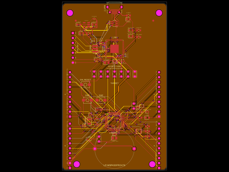 More from this authorShiboSoftwareDev/lp-msp430fr2476This design implements a microcontroller-based development board featuring an MSP430FR2476 target MCU with associated power regulation, USB host interface with ESD protection, multiple headers for peripherals and BoosterPacks, and integrated status LEDs and sensors.
 Similar packageaura/diy-power-delivery-triggerThis hardware design implements a USB Type-C port with supporting power management and signal conditioning components, including a USB-C connector, a FUSB302 USB-C port controller, ESD protection diodes, a buck converter for 3.3V power regulation, an STM32 microcontroller for control and processing, an RGB LED indicator, push button, terminal block connections, and associated filtering and support components.
 Discover something newrushabhcodes/ESP32-E-ReaderThis code defines the physical layout and schematic wiring of an ESP32-based e-reader device, including various surface-mount components such as connectors, ICs, resistors, capacitors, inductors, diodes, pushbuttons, and an antenna, with precise PCB placement and interconnection details.