imrishabh18/pedometer
This code defines and assembles a simple radio receiver hardware circuit using specific imported capacitors, inductors, RF connectors, and oscillator components with precise footprints and schematic attributes.
- Version
- 1.1.3
- License
- unset
- Stars
- 0
docs/design.md
# Stride Rev A design record

## Baseline

40 × 38 mm, four-layer, 1.0 mm host PCB; external 35 × 20 mm Adafruit 4440 OLED; rechargeable **protected 100 mAh, 1S, 4.2 V Li-ion/LiPo** pack with a thermistor attached to the cell. The PCB area is 1520 mm², enlarged from the prior 1088 mm² bare-chip layout to separate the power, sensing and connector regions and give the autorouter legal copper corridors. The external display still determines one enclosure dimension. This is a first engineering revision, with final mechanical envelope, cell part number and enclosure still open. The battery and OLED must stay out of the ANT1 antenna region. Weeks of operation require the screen to remain off between short button presses.

## Architecture

```mermaid
flowchart LR
  USB[Regulated 5 V charge contacts] --> PM[BQ25150 power path + charger]
  BAT[Protected 100 mAh cell] <--> FG[BQ27427 high-side gauge]
  FG <--> PM
  NTC[Cell-mounted 10k NTC] --> PM
  PM -->|PMID| LDO[TPS7A02 / 2.5 V]
  LDO --> MCU[Bare CC2340R5 QFN24]
  LDO --> ACC[BMA400 step counter]
  PM -->|Switched 3.3 V LSLDO| OLED[128 × 32 OLED]
  MCU <-->|2.5 V I2C| ACC
  MCU <-->|I2C| PM
  MCU <-->|I2C| FG
  MCU <-->|I2C| XL[PCA9306 + reset isolation]
  XL <-->|3.3 V I2C| OLED
  MCU <-->|BLE| PHONE[Phone / computer]
```

**MCU:** U1 is the bare CC2340R52E0RGER QFN24. The board now provides its own DC/DC network, 48 MHz crystal, reset network, RF low-pass filter and separate Johanson ceramic antenna. See [bare-chip circuit details](bare-cc2340r5.md).

**Step counting:** BMA400 performs the step algorithm while the MCU sleeps. Normal mode, 100 Hz, OSR 0 is the initial configuration; do not switch to 25 Hz low-power mode and assume the same counting function. Firmware polls every 60 seconds and on a button press, avoiding a processor wake on every step. Select wrist or non-wrist coefficients at build/integration time, then validate against manually counted walks. INT1 is wired for later activity/tap experiments and configured open-drain even when unmapped. [Bosch datasheet](https://www.bosch-sensortec.com/media/boschsensortec/downloads/datasheets/bst-bma400-ds000.pdf).

**Charging:** BQ25150 supplies the system through PMID. Firmware requests 4.20 V, 20 mA fast charge, 2.5 mA precharge and 2 mA termination; temperature monitoring and a 12-hour safety timer stay enabled. R3 = 499 Ω constrains the current code, approximately 21.25 mA in the selected 1.25 mA range before tolerance. Selecting the other range doubles this limit, so it is not an unconditional 20 mA hardware cap. The POR setting is 10 mA. A compatible cell must explicitly permit these settings. Use a 10 kΩ NTC with the curve required by TI's TS thresholds, attached to the battery, from J1.3 to J1.2; R4 provides the 10 kΩ parallel bias resistor explicitly required by the BQ25150 TS circuit. Charger protection does not replace a pack protection circuit. [BQ25150 datasheet](https://www.ti.com/lit/ds/symlink/bq25150.pdf).

**Gauge:** BQ27427 senses the battery on the positive side: J1 PACK+ → BAT → internal sense element → SRX → charger BAT. All system loads take power downstream through PMID so their charge passes through the gauge. BIN uses 10 kΩ to ground for an embedded pack. Its VDD is a decoupling-only internal rail. TI lists 100 mAh as the minimum supported capacity. Smaller batteries need a new gauging decision. [TI product page](https://www.ti.com/product/BQ27427), [gauge datasheet](https://www.ti.com/lit/ds/symlink/bq27427.pdf).

**Power rails and display isolation:** A separate TPS7A0225 supplies 2.5 V continuously; the charger's LSLDO supplies only the OLED. The PMIC resets with LSLDO enabled at 1.8 V. Q1 and R11 therefore hold the PCA9306 translator disabled during MCU reset. Firmware first disables LSLDO, then configures 3.3 V. To show the screen, enable 3.3 V, wait, release isolation, and initialize SSD1306. To turn off, isolate the bus first, then remove power. This prevents the unpowered or undervoltage display from clamping the main I2C bus. R10 is the PCA9306 200 kΩ bias resistor; VREF2 and EN are tied together on its low-current bias node, not directly to 3.3 V. [TPS7A02](https://www.ti.com/lit/ds/symlink/tps7a02.pdf), [PCA9306](https://www.ti.com/lit/ds/symlink/pca9306.pdf), [Adafruit OLED](https://www.adafruit.com/product/4440).

**Button:** MR is pulled toward battery voltage inside the PMIC. It never connects directly to a CC2340 GPIO. PG is programmed to reflect MR as an open-drain signal pulled to 2.5 V. A long press retains the PMIC hardware-reset behavior. LP is driven high for an I2C transaction and low afterward; firmware allows 2 ms for wake.

**32 kHz clock:** ABS07, 7 pF load rating, with initial 12 pF and 15 pF C0G capacitors. These are starting values, not a crystal characterization result. Tune for the PCB and pin parasitics and check oscillator startup across temperature and battery voltage. [Abracon](https://abracon.com/Resonators/ABS07.pdf), [TI reference discussion](https://e2e.ti.com/support/wireless-connectivity/bluetooth-group/bluetooth/f/bluetooth-forum/1381327/lp-em-cc2340r5-supported-crystal-load-capacitance-suggest-capacitor-value).

## Layout and assembly intent

- Top: all components and local decoupling. Inner1: ground reference; no signal routes. Inner2: signal/power routing. Bottom: routing plus ground fill.
- Minimum requested trace width 0.10 mm and copper clearance 0.075 mm; minimum via drill 0.15 mm and land 0.30 mm. These require the chosen fabricator's approval. The autorouter creates all traces and vias. A geometry-based routing stage identifies enclosed BGA balls and QFN center pads, and requests terminal vias only when enabled; it contains no component-specific coordinates. A planning envelope keeps routes out of the nominal QFN pin gaps. The adapter includes the pad-side endpoints of generated terminal vias for tscircuit connectivity checks. No explicit vias or route waypoints are defined. Review its generated escapes with the fabricator. Any generated via-in-pad must be filled and capped; ordinary open vias underneath solder balls are unsuitable.
- The crystal nets route first on top copper, with their native zero-via and length checks enabled. The remaining routing treats that copper as fixed. An automatic clearance stage moves free generated vias and their adjoining wire segments only when the resulting geometry clears other nets and the board outline; pad terminals and prior clock copper remain fixed. The final native DRC and Gerber shorts checks run after this stage, with no suppressed diagnostics or reduced board clearances.
- U2 is 0.4 mm pitch DSBGA; U3 is 0.5 mm pitch DSBGA. Plan professional paste/reflow assembly and X-ray inspection. Imported pad geometry, solder-mask apertures, stencil and pick-and-place rotations require package/assembler verification.
- J1/J3/J4 are top-entry JST-SH connectors for the 3-pin battery/NTC, 4-pin OLED and 5-pin SWD interfaces. J2 is a side-entry USB-C 6P receptacle for 5 V charging, with separate 5.1 kΩ CC pull-downs and a VBUS transient clamp. Its four plated mounting slots connect to ground. Reserve space above the JST connectors for housings/wire bends and outside the top board edge for the USB-C plug. Two 2.2 mm mounting holes are centered at (12.3, 11.3) mm and (−12.3, −11.3) mm, relative to the board center. Use the current placement coordinates for the enclosure.
- Decoupling values are nominal. In particular, check the effective capacitance of PMID, PMIC VDD, gauge VDD and OLED LDO capacitors at operating bias against the datasheets.

The CAD validation report governs release status. Connectivity intent alone is not a manufacturing signoff. The final battery, temperature thresholds, DSBGA assembly process, antenna performance and measured power are required prototype decisions.
Related Packages
 More from this authorimrishabh18/test-pcmThis code defines a 10mm by 10mm electronic circuit board containing a single pin-row chip with an associated 3D CAD model of the "MachineContactMedium" component.
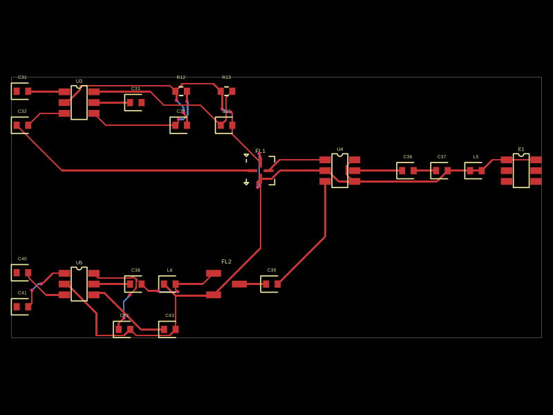 Similar packageMustafaMulla29/CC3235SF-tsxThis code defines a PCB layout with RF front-end components including RF switches (RTC6608OSP), band-pass filters, a diplexer, matching capacitors and inductors, and an antenna, all arranged to match a specific schematic for high-frequency radio signal routing.
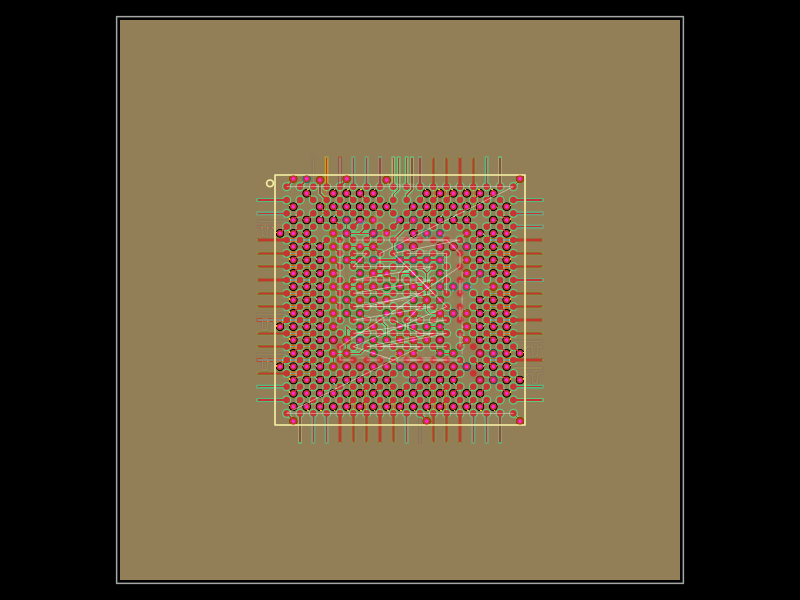 Discover something new0hmX/am3352This code defines a six-layer printed circuit board (PCB) design with a TI AM3352 microprocessor package, including precise pin mapping, power plane definition, fixed component placement, and PCB layout visualization.